Board Design & Layout
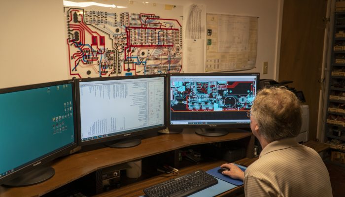
This service is the process of turning design schematics into a PCB layout. The layout is what ends up becoming the circuit board we manufacture, so it’s a very critical piece of the process. Our PCB Designer has over 40 years of experience creating board layouts and actually designed the light table PCB hanging on the wall in the photo above. There are many ways to design the same board, but each design will end up acting just a little different from the other due to outside electrical noise, etc. Here, at Thomas Instrumentation, we prefer to hand lay out the board by manually placing components, setting the width & path of traces, and creating ground and power planes. We find this method gives us better control over design characteristics such as EMI noise reduction, heat dissipation, antennas, grounding, efficiency, reliability, and more.
PCB Layout from Design Schematics
Typically, our customers hire us for the complete engineering design process. When that happens, we have the luxury of laying out the PCB from our own schematics. However, we do occasionally work from other company’s schematics. It just takes a bit longer as we have to copy those over into our system. Regardless of the starting point, we start building the layout by asking customers to define the physical constraints of their product. These include but are not limited to: PCB dimensions, mounting hole locations, methods of connection to other boards or peripherals, and even weight. Once that information is obtained, then we complete the PCB layout, review the design characteristics mentioned earlier, and package the information for release to our PCB houses.
PCB Layout from Existing Layouts
Over the years, we’ve found that companies often have their product’s Gerber files (PCB layout) and nothing else. They’ve come to us with only these files and ask if we can reproduce and/or modify their existing layout. When this happens, we either import the files, if compatible, or we manually copy the layout into our system. Once it’s in our system, we prefer to do an in-depth review of the layout. This gives us time to verify the design characteristics mentioned earlier were properly met. Once we’re satisfied with the design, we package the information for release.
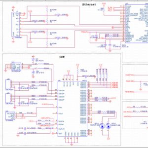
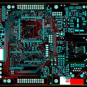
Luckily, the days of light table PCB layouts are long gone. Our PCB Designer has been using the Cadence OrCAD product line for close to 30 years. We first use OrCAD Capture to create our digital schematics and bill of materials (BOMs). Then, we use the OrCAD Layout program to develop the Gerber files necessary for purchasing actual PCBs. There are also two layers of error checking to this process. OrCAD itself has an automated error checking feature and our PCB houses’ always perform an error check. It is only after our design passes both tests that the board moves into actual production manufacturing.
Since Thomas Instrumentation almost never designs a PCB without then manufacturing it, our technicians typically start creating our internal production files.