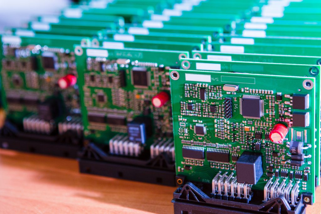
Board Design & Layout

Thomas Instrumentation provides pcb layout services that turn your schematic and requirements into a manufacturable, production-ready board. As part of our Electronics (PCB) Design capability, our pcb layout design services focus on placement, constraint-driven routing, and clear releases that help prototypes move forward with fewer re-spins. You get engineer-to-engineer collaboration across revisions.

What Board Design & Layout Means

Board design and layout is the physical implementation of your circuit: component placement, trace routing, stack-up planning, and verification checks that become fabrication and assembly data. Smart layout decisions support controlled impedance routing when required, crosstalk control, and EMI preparedness while keeping the design practical to build repeatedly.

Manufacturing Process of Custom PCB Board.png

What’s Included in Our PCB Layout Services

  1. Stack-up definition and layer planning aligned to performance and manufacturability
  2. Design rules and constraints, including clearances and impedance targets when needed
  3. Component placement optimized for signal flow, assembly access, and test strategy
  4. Routing with attention to return paths, noise reduction, and critical nets
  5. Verification passes, including DRC plus What Is Design for Manufacturability (DFM) in PCB Design? alignment with real build capabilities
  6. Engineering reviews to confirm intent, interfaces, and revision changes
A bustling smart city skyline overlaid with glowing network connectivity lines.

Deliverables You Receive

You receive a build-ready file set so your team can fabricate and assemble without guesswork:

  • Gerbers and drill files
  • Assembly outputs such as BOM and placement data
  • Fabrication and assembly notes for constraints, connectors, and interfaces
  • A release package prepared to support prototyping and ECOs

Our Layout Workflow

Requirements capture, mechanical constraints, and interface priorities
Library and footprint preparation, rule setup, and stack-up definition
Placement, routing, and review with DRC and DFM checks
Release of manufacturing outputs and support through prototype builds with Electronics Manufacturing Services (EMS) resources when appropriate

Designed for Industrial, Laboratory, and Appliance Electronics

We deliver circuit board layout services for Industrial controls, laboratory and biopharmaceutical equipment, and appliance platforms. For a laboratory-focused example, Why Pharmaceutical Lab OEMs Choose U.S.-Based PCB Partners for High-Precision Device Manufacturing explains why build readiness and documentation matter when uptime and serviceability are priorities.

Why choose Thomas Instrumentation?

customer centric approach

Expertise

Decades of extensive experience in PCB design across diverse industries.

customization 1

Customization

Tailored solutions expertly crafted to meet your specific project requirements.

quality and compliance

Quality assurance

Comprehensive and rigorous testing, quality control for every design.

innovation 1 1 scaled e1727854680545

Innovation

A commitment to incorporating the latest technology and innovations.

Board Design & Layout FAQs

What do you need to start a PCB layout?

A schematic, key mechanical constraints, connector locations, and any performance targets help us set rules quickly.

Yes. We deliver Gerbers, drill data, and assembly outputs in a clear release package.

Yes. We support revisions, ECOs, and lifecycle updates as designs evolve.